Media Summary: PCB Design Tutorial_28 Orcad Pcb Editor Custom Part 02 Footprint Creation Dimension Update PCB Design Tutorial_38 Orcad Pcb Editor Netlist Import And Error Correction 02 Sometimes we might not find schematic symbol for some components in our
Pcb Design Tutorial 38 Orcad - Detailed Analysis & Overview
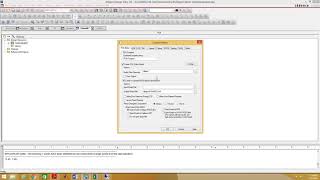
PCB Design Tutorial_28 Orcad Pcb Editor Custom Part 02 Footprint Creation Dimension Update PCB Design Tutorial_38 Orcad Pcb Editor Netlist Import And Error Correction 02 Sometimes we might not find schematic symbol for some components in our PCB Design Tutorial_25 Orcad Pcb Editor Custom Part 01 Footprint Creation In this video it is shown, how to create a through hole DIP and a SMD SOIC footprint using the 'Package Symbol Wizard' in ... PCB Design Tutorial_57 Orcad Pcb Editor Fabrication Drawing Creation
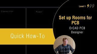
PCB Design Tutorial_17 Orcad Sch Part Properties Edit Professor Saeid Moslehpour Video by: Jeff Roberts, Gary Claus, and Sam Alexander This video covers: -Creating component ... In this video, we'll provide an in-depth explanation on how to configure and create rooms for component placement for efficient ... ... we used go to the project folder select the design file go to tools select create netlist select create or update ... to do a complete PCB using orchad um so we will be covering three different software in orad the the capture uh