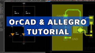
Media Summary: PCB Design Tutorial_57 Orcad Pcb Editor Fabrication Drawing Creation PCB Design Tutorial_51 Orcad Pcb Editor Design Rule Check Drc Cleanup PCB Design Tutorial_17 Orcad Sch Part Properties Edit

Pcb Design Tutorial 57 Orcad - Detailed Analysis & Overview

PCB Design Tutorial_57 Orcad Pcb Editor Fabrication Drawing Creation PCB Design Tutorial_51 Orcad Pcb Editor Design Rule Check Drc Cleanup PCB Design Tutorial_17 Orcad Sch Part Properties Edit PCB Design Tutorial_25 Orcad Pcb Editor Custom Part 01 Footprint Creation PCB Design Tutorial_59 Orcad Pcb Editor Assembly Files Generation Gencad Pick&place Files PCB Design Tutorial_23 Orcad Pcb Editor Library Path Setting

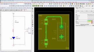
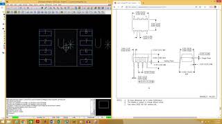
PCB Design Tutorial_52 Orcad Pcb Editor Artwork Film Setup For everyone who would like to learn how to start with In this video it is shown, how to create a through hole DIP and a SMD SOIC footprint using the 'Package Symbol Wizard' in ... It is always preferable to create power and ground planes instead of routing traces, for intended

Photo Gallery

PCB Design Tutorial_57 Orcad Pcb Editor Fabrication Drawing Creation
PCB Design Tutorial_51 Orcad Pcb Editor Design Rule Check Drc Cleanup
Tutorial OrCAD and Cadence Allegro PCB Editor | 2022 | Step by Step | For Beginners
Complete PCB Design Course in OrCAD and Allegro 17.4 | OrCAD & Allegro PCB Design by LtlBiTech
PCB Design Tutorial_17 Orcad Sch Part Properties Edit
PCB Design Tutorial_25 Orcad Pcb Editor Custom Part 01 Footprint Creation
PCB Design Tutorial_59 Orcad Pcb Editor Assembly Files Generation Gencad Pick&place Files
PCB Design Tutorial_23 Orcad Pcb Editor Library Path Setting
PCB Design Tutorial_52 Orcad Pcb Editor Artwork Film Setup
Starting with OrCAD and Cadence Allegro PCB - Tutorial for Beginners
Orcad PCB Design Tutorial - 10 Create smd and through hole footprint
Cadence OrCad PCB Editor 17.4 (Complete board layout in 30 min)
View Detailed Profile
PCB Design Tutorial_57 Orcad Pcb Editor Fabrication Drawing Creation

PCB Design Tutorial_57 Orcad Pcb Editor Fabrication Drawing Creation

PCB Design Tutorial_57 Orcad Pcb Editor Fabrication Drawing Creation

PCB Design Tutorial_51 Orcad Pcb Editor Design Rule Check Drc Cleanup

PCB Design Tutorial_51 Orcad Pcb Editor Design Rule Check Drc Cleanup

PCB Design Tutorial_51 Orcad Pcb Editor Design Rule Check Drc Cleanup

Tutorial OrCAD and Cadence Allegro PCB Editor | 2022 | Step by Step | For Beginners

Tutorial OrCAD and Cadence Allegro PCB Editor | 2022 | Step by Step | For Beginners

After this

Complete PCB Design Course in OrCAD and Allegro 17.4 | OrCAD & Allegro PCB Design by LtlBiTech

Complete PCB Design Course in OrCAD and Allegro 17.4 | OrCAD & Allegro PCB Design by LtlBiTech

To join our professional online course: https://pradeip009.wixsite.com/

PCB Design Tutorial_17 Orcad Sch Part Properties Edit

PCB Design Tutorial_17 Orcad Sch Part Properties Edit

PCB Design Tutorial_17 Orcad Sch Part Properties Edit

PCB Design Tutorial_25 Orcad Pcb Editor Custom Part 01 Footprint Creation

PCB Design Tutorial_25 Orcad Pcb Editor Custom Part 01 Footprint Creation

PCB Design Tutorial_25 Orcad Pcb Editor Custom Part 01 Footprint Creation

PCB Design Tutorial_59 Orcad Pcb Editor Assembly Files Generation Gencad Pick&place Files

PCB Design Tutorial_59 Orcad Pcb Editor Assembly Files Generation Gencad Pick&place Files

PCB Design Tutorial_59 Orcad Pcb Editor Assembly Files Generation Gencad Pick&place Files

PCB Design Tutorial_23 Orcad Pcb Editor Library Path Setting

PCB Design Tutorial_23 Orcad Pcb Editor Library Path Setting

PCB Design Tutorial_23 Orcad Pcb Editor Library Path Setting

PCB Design Tutorial_52 Orcad Pcb Editor Artwork Film Setup

PCB Design Tutorial_52 Orcad Pcb Editor Artwork Film Setup

PCB Design Tutorial_52 Orcad Pcb Editor Artwork Film Setup

Starting with OrCAD and Cadence Allegro PCB - Tutorial for Beginners

Starting with OrCAD and Cadence Allegro PCB - Tutorial for Beginners

For everyone who would like to learn how to start with

Orcad PCB Design Tutorial - 10 Create smd and through hole footprint

Orcad PCB Design Tutorial - 10 Create smd and through hole footprint

In this video it is shown, how to create a through hole DIP and a SMD SOIC footprint using the 'Package Symbol Wizard' in ...

Cadence OrCad PCB Editor 17.4 (Complete board layout in 30 min)

Cadence OrCad PCB Editor 17.4 (Complete board layout in 30 min)

Complete

10 - Design With OrCAD: Copper

10 - Design With OrCAD: Copper

It is always preferable to create power and ground planes instead of routing traces, for intended