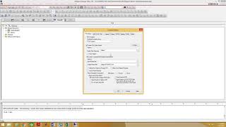
Media Summary: ... we used go to the project folder select the In this series. Adam Fuchs, Product Engineer at Welcome to Raan Dayzz This video shows How to
Orcad Pcb Design Tutorial 3 - Detailed Analysis & Overview
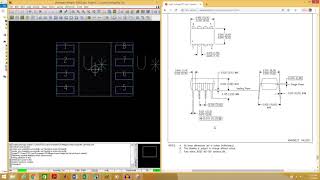
... we used go to the project folder select the In this series. Adam Fuchs, Product Engineer at Welcome to Raan Dayzz This video shows How to In this video it is shown, how to create a through hole DIP and a SMD SOIC footprint using the 'Package Symbol Wizard' in ... PCB Design Tutorial_31 Orcad Pcb Editor Custom Part 03 Footprint Creation Dimension Update Playstore App for the channel: For GATE 2018 EC ...
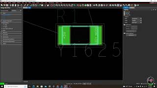
In this video, we'll provide an in-depth explanation on creating copper planes in