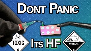
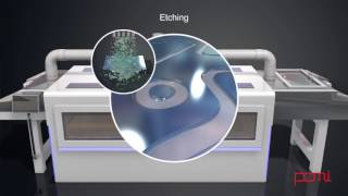
Media Summary: We have now plated the panel with 25 microns of copper through the hole and an additional 25 -- 30 microns on the tracks and ... We remove the unwanted copper using a powerful alkaline solution to dissolve (or Victory provides one-stop PCB manufacturing and assembly services. We will help you understand how exactly a PCB is made.

Part 15 Etch Outer Layers - Detailed Analysis & Overview

We have now plated the panel with 25 microns of copper through the hole and an additional 25 -- 30 microns on the tracks and ... We remove the unwanted copper using a powerful alkaline solution to dissolve (or Victory provides one-stop PCB manufacturing and assembly services. We will help you understand how exactly a PCB is made. Support me on Patreon: In this video I evaluate three easy-to-obtain sources for ... Inkscape is professional, free, open source Vector Graphics software. You can download it today, on Windows/Linux/Mac at: ... The class prop allows you to choose which elements in a component can receive custom, stylable classes from the

Welcome to Scale Model Basics: Dos and don'ts with photo-

Photo Gallery

Part 15 - Etch outer layers
Part 5 - Etch inner layers
Part 13 - Image the outer layers
outer layers etching
How to etch the outer layer of the PCBs?
Outer layer etch line&AOI—— PCB Manufacturing & Assembly Inside Factory in China- VictoryPCB.com
Using Hydrofluoric Acid to Etch Oxide Layers
Faraday Printed Circuits - Etch Inner Layers
Etching Process
Inkscape Lesson 15 - Using Layers
Etch Class Prop (V1) - Making Component Elements Stylable From the Outside
Scale Model Basics: Dos and don'ts with photo-etched metal parts
View Detailed Profile
Part 15 - Etch outer layers

Part 15 - Etch outer layers

We have now plated the panel with 25 microns of copper through the hole and an additional 25 -- 30 microns on the tracks and ...

Part 5 - Etch inner layers

Part 5 - Etch inner layers

We remove the unwanted copper using a powerful alkaline solution to dissolve (or

Part 13 - Image the outer layers

Part 13 - Image the outer layers

We image the

outer layers etching

outer layers etching

outer layers etching

How to etch the outer layer of the PCBs?

How to etch the outer layer of the PCBs?

How to

Outer layer etch line&AOI—— PCB Manufacturing & Assembly Inside Factory in China- VictoryPCB.com

Outer layer etch line&AOI—— PCB Manufacturing & Assembly Inside Factory in China- VictoryPCB.com

Victory provides one-stop PCB manufacturing and assembly services. We will help you understand how exactly a PCB is made.

Using Hydrofluoric Acid to Etch Oxide Layers

Using Hydrofluoric Acid to Etch Oxide Layers

Support me on Patreon: https://www.patreon.com/projectsinflight In this video I evaluate three easy-to-obtain sources for ...

Faraday Printed Circuits - Etch Inner Layers

Faraday Printed Circuits - Etch Inner Layers

Utilising Macdermind Chemistry, inner

Etching Process

Etching Process

Etching Process

Inkscape Lesson 15 - Using Layers

Inkscape Lesson 15 - Using Layers

Inkscape is professional, free, open source Vector Graphics software. You can download it today, on Windows/Linux/Mac at: ...

Etch Class Prop (V1) - Making Component Elements Stylable From the Outside

Etch Class Prop (V1) - Making Component Elements Stylable From the Outside

The class prop allows you to choose which elements in a component can receive custom, stylable classes from the

Scale Model Basics: Dos and don'ts with photo-etched metal parts

Scale Model Basics: Dos and don'ts with photo-etched metal parts

Welcome to Scale Model Basics: Dos and don'ts with photo-

Outer layer etch line&AOI——PCB Manufacturing & Assembly Inside Factory in China- VictoryPCB.com

Outer layer etch line&AOI——PCB Manufacturing & Assembly Inside Factory in China- VictoryPCB.com

Victory provides one-stop PCB manufacturing and assembly services. We will help you understand how exactly a PCB is made.