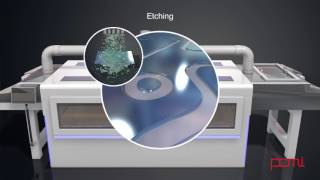
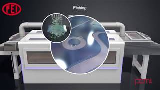
Media Summary: We have now plated the panel with 25 microns of copper through the hole and an additional 25 -- 30 microns on the tracks and ... We remove the unwanted copper using a powerful alkaline solution to dissolve (or Victory provides one-stop PCB manufacturing and assembly services. We will help you understand how exactly a PCB is made.

Outer Layers Etching - Detailed Analysis & Overview

We have now plated the panel with 25 microns of copper through the hole and an additional 25 -- 30 microns on the tracks and ... We remove the unwanted copper using a powerful alkaline solution to dissolve (or Victory provides one-stop PCB manufacturing and assembly services. We will help you understand how exactly a PCB is made. Links: - The Asianometry Newsletter: - Patreon: - Threads: ... PCMI produced, animated process of Chemical

Photo Gallery

Etching Process in PCB Manufacturing
Part 15 - Etch outer layers
outer layers etching
PCB Manufacturing Process: Outer Layer Etching
8. Outer layers Etching
Part 5 - Etch inner layers
PCB Outer Layer Pre-treatment - Ensuring Surface Readiness for Circuit Formation.
Outer layer etch line&AOI—— PCB Manufacturing & Assembly Inside Factory in China- VictoryPCB.com
Etching Process
Faraday Printed Circuits - Etch Inner Layers
Etch: Lithography's Unheralded Sibling
The Etching Process
View Detailed Profile
Etching Process in PCB Manufacturing

Etching Process in PCB Manufacturing

The

Part 15 - Etch outer layers

Part 15 - Etch outer layers

We have now plated the panel with 25 microns of copper through the hole and an additional 25 -- 30 microns on the tracks and ...

outer layers etching

outer layers etching

outer layers etching

PCB Manufacturing Process: Outer Layer Etching

PCB Manufacturing Process: Outer Layer Etching

Outer layer etching

8. Outer layers Etching

8. Outer layers Etching

Outer layers Etching

Part 5 - Etch inner layers

Part 5 - Etch inner layers

We remove the unwanted copper using a powerful alkaline solution to dissolve (or

PCB Outer Layer Pre-treatment - Ensuring Surface Readiness for Circuit Formation.

PCB Outer Layer Pre-treatment - Ensuring Surface Readiness for Circuit Formation.

PCB

Outer layer etch line&AOI—— PCB Manufacturing & Assembly Inside Factory in China- VictoryPCB.com

Outer layer etch line&AOI—— PCB Manufacturing & Assembly Inside Factory in China- VictoryPCB.com

Victory provides one-stop PCB manufacturing and assembly services. We will help you understand how exactly a PCB is made.

Etching Process

Etching Process

Etching Process

Faraday Printed Circuits - Etch Inner Layers

Faraday Printed Circuits - Etch Inner Layers

Utilising Macdermind Chemistry, inner

Etch: Lithography's Unheralded Sibling

Etch: Lithography's Unheralded Sibling

Links: - The Asianometry Newsletter: https://www.asianometry.com - Patreon: https://www.patreon.com/Asianometry - Threads: ...

The Etching Process

The Etching Process

PCMI produced, animated process of Chemical

PCB Manufacturer China丨Outer Layer Image SES (Strip film - etching - strim Tin)

PCB Manufacturer China丨Outer Layer Image SES (Strip film - etching - strim Tin)

PCB Manufacturer China丨