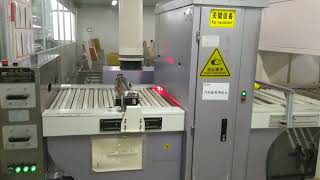
Media Summary: Victory provides one-stop PCB manufacturing and assembly services. We will help you understand how exactly a PCB is made. We have now plated the panel with 25 microns of copper through the hole and an additional 25 -- 30 microns on the tracks and ... Join us in this comprehensive tutorial as we walk you through 33 detailed steps of producing a reliable multilayer printed circuit ...

Outer Layer Etch Line Aoi - Detailed Analysis & Overview

Victory provides one-stop PCB manufacturing and assembly services. We will help you understand how exactly a PCB is made. We have now plated the panel with 25 microns of copper through the hole and an additional 25 -- 30 microns on the tracks and ... Join us in this comprehensive tutorial as we walk you through 33 detailed steps of producing a reliable multilayer printed circuit ... Discover how Automated Optical Inspection ( To inspect defects of coating, such as excessive, insufficient, splash, bubble etc.

Photo Gallery

Outer layer etch line&AOI—— PCB Manufacturing & Assembly Inside Factory in China- VictoryPCB.com
Printed Circuit Board Manufacturer丨Outer Layer Image AOI
Part 15 - Etch outer layers
Outer layer AOI | How to make a PCB step 6.5
Etching Process in PCB Manufacturing
PCB Manufacturing Process: Outer Layer Etching
PCB Outer Layer Line AOI - Ensuring Quality and Accuracy of Circuit Traces.
PCB Manufacturer China丨Outer Layer Image SES (Strip film - etching - strim Tin)
Online AOI For Multi-layer PCB Inner Layer After Etching
outer layers etching
Inner Layer AOI
How AOI Guarantees Precision After PCB Etching
View Detailed Profile
Outer layer etch line&AOI—— PCB Manufacturing & Assembly Inside Factory in China- VictoryPCB.com

Outer layer etch line&AOI—— PCB Manufacturing & Assembly Inside Factory in China- VictoryPCB.com

Victory provides one-stop PCB manufacturing and assembly services. We will help you understand how exactly a PCB is made.

Printed Circuit Board Manufacturer丨Outer Layer Image AOI

Printed Circuit Board Manufacturer丨Outer Layer Image AOI

Printed Circuit Board Manufacturer丨

Part 15 - Etch outer layers

Part 15 - Etch outer layers

We have now plated the panel with 25 microns of copper through the hole and an additional 25 -- 30 microns on the tracks and ...

Outer layer AOI | How to make a PCB step 6.5

Outer layer AOI | How to make a PCB step 6.5

Join us in this comprehensive tutorial as we walk you through 33 detailed steps of producing a reliable multilayer printed circuit ...

Etching Process in PCB Manufacturing

Etching Process in PCB Manufacturing

The

PCB Manufacturing Process: Outer Layer Etching

PCB Manufacturing Process: Outer Layer Etching

Outer layer etching

PCB Outer Layer Line AOI - Ensuring Quality and Accuracy of Circuit Traces.

PCB Outer Layer Line AOI - Ensuring Quality and Accuracy of Circuit Traces.

PCB

PCB Manufacturer China丨Outer Layer Image SES (Strip film - etching - strim Tin)

PCB Manufacturer China丨Outer Layer Image SES (Strip film - etching - strim Tin)

PCB Manufacturer China丨

Online AOI For Multi-layer PCB Inner Layer After Etching

Online AOI For Multi-layer PCB Inner Layer After Etching

Online

outer layers etching

outer layers etching

outer layers etching

Inner Layer AOI

Inner Layer AOI

7 Inner

How AOI Guarantees Precision After PCB Etching

How AOI Guarantees Precision After PCB Etching

Discover how Automated Optical Inspection (

Inline PCBA AOI For Coating:AIS 50X-C-HW

Inline PCBA AOI For Coating:AIS 50X-C-HW

To inspect defects of coating, such as excessive, insufficient, splash, bubble etc.