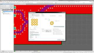
Media Summary: Multidisciplinary product creation powered by your unconstrained network. Work concurrently across design, sourcing, and ... Basics, guidelines, and best practices for vias in PCB designs. From sizing, to placement, to transfer and Chris shows the steps explained in this KiCad.info Forum post for the visual learners: ...

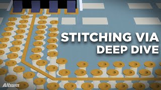
Zone Via Stitching - Detailed Analysis & Overview

Multidisciplinary product creation powered by your unconstrained network. Work concurrently across design, sourcing, and ... Basics, guidelines, and best practices for vias in PCB designs. From sizing, to placement, to transfer and Chris shows the steps explained in this KiCad.info Forum post for the visual learners: ...

Photo Gallery

Zone Via Stitching
How and When to Use Via Stitching
Stitching Via Deep Dive | PCB Layout
(Sponsored) PCB Vias 101 - Phil's Lab #77
How to Use Via Shielding and Stitching Tools in Altium Designer
Altium Designer 14 - Regional Via Stitching
Via Stitching and Shielding | Altium Designer 17 Advanced | Module 11
To Pour or Not To Pour | Copper Pour in PCB Design
How GND VIAs Improve Your PCB Layout
Stitching Vias
KiCad 4.0 - Via Stitching In KiCad (without traces)
17 KiCad Tutorial: Fill Zones Mastery - Adding GND to Fill Zones and Incorporating Vias
View Detailed Profile
Zone Via Stitching

Zone Via Stitching

Via stitching

How and When to Use Via Stitching

How and When to Use Via Stitching

Via stitching

Stitching Via Deep Dive | PCB Layout

Stitching Via Deep Dive | PCB Layout

Multidisciplinary product creation powered by your unconstrained network. Work concurrently across design, sourcing, and ...

(Sponsored) PCB Vias 101 - Phil's Lab #77

(Sponsored) PCB Vias 101 - Phil's Lab #77

Basics, guidelines, and best practices for vias in PCB designs. From sizing, to placement, to transfer and

How to Use Via Shielding and Stitching Tools in Altium Designer

How to Use Via Shielding and Stitching Tools in Altium Designer

Multidisciplinary product creation powered by your unconstrained network. Work concurrently across design, sourcing, and ...

Altium Designer 14 - Regional Via Stitching

Altium Designer 14 - Regional Via Stitching

... set individually for each

Via Stitching and Shielding | Altium Designer 17 Advanced | Module 11

Via Stitching and Shielding | Altium Designer 17 Advanced | Module 11

Multidisciplinary product creation powered by your unconstrained network. Work concurrently across design, sourcing, and ...

To Pour or Not To Pour | Copper Pour in PCB Design

To Pour or Not To Pour | Copper Pour in PCB Design

He explores

How GND VIAs Improve Your PCB Layout

How GND VIAs Improve Your PCB Layout

See how a

Stitching Vias

Stitching Vias

Save parameters for

KiCad 4.0 - Via Stitching In KiCad (without traces)

KiCad 4.0 - Via Stitching In KiCad (without traces)

Chris shows the steps explained in this KiCad.info Forum post for the visual learners: ...

17 KiCad Tutorial: Fill Zones Mastery - Adding GND to Fill Zones and Incorporating Vias

17 KiCad Tutorial: Fill Zones Mastery - Adding GND to Fill Zones and Incorporating Vias

KiCad Tutorial: Fill

KiCad 5.0 - Via Stitching

KiCad 5.0 - Via Stitching

Via stitching