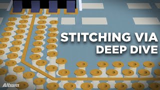
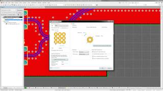
Media Summary: Multidisciplinary product creation powered by your unconstrained network. Work concurrently across design, sourcing, and ... Crosstalk and EMI issues are huge sources of concern when designing for high-speed applications. One method developed to ... Basics, guidelines, and best practices for vias in PCB designs. From sizing, to placement, to transfer and

Stitching Vias - Detailed Analysis & Overview

Multidisciplinary product creation powered by your unconstrained network. Work concurrently across design, sourcing, and ... Crosstalk and EMI issues are huge sources of concern when designing for high-speed applications. One method developed to ... Basics, guidelines, and best practices for vias in PCB designs. From sizing, to placement, to transfer and In this video, Zach Peterson explains why differential vias need Here is an illustration of how badly single-ended via needs Commenting on a PCB Layout done by a junior engineer. ------------------------------------------------------ Would you like to support me in ...

Photo Gallery

Stitching Via Deep Dive | PCB Layout
How and When to Use Via Stitching
Eliminate Crosstalk and EMI with Via Stitching in Altium Designer
Comparison of two stitching vias placement options for differential vias
How to Use Via Shielding and Stitching Tools in Altium Designer
(Sponsored) PCB Vias 101 - Phil's Lab #77
How GND VIAs Improve Your PCB Layout
How Many Stitching Vias Does Your PCB Need? #signalintegrity #pcbdesign #altiumdesigner #kicad
Altium Designer 14 - Regional Via Stitching
Via Stitching and Shielding | Altium Designer 17 Advanced | Module 11
Localization of differential and common mode in differential vias with two stitching vias
Power flow in single-ended via without and with 2 stitching vias at 10 GHz
View Detailed Profile
Stitching Via Deep Dive | PCB Layout

Stitching Via Deep Dive | PCB Layout

Multidisciplinary product creation powered by your unconstrained network. Work concurrently across design, sourcing, and ...

How and When to Use Via Stitching

How and When to Use Via Stitching

Via stitching

Eliminate Crosstalk and EMI with Via Stitching in Altium Designer

Eliminate Crosstalk and EMI with Via Stitching in Altium Designer

Crosstalk and EMI issues are huge sources of concern when designing for high-speed applications. One method developed to ...

Comparison of two stitching vias placement options for differential vias

Comparison of two stitching vias placement options for differential vias

Differential vias need

How to Use Via Shielding and Stitching Tools in Altium Designer

How to Use Via Shielding and Stitching Tools in Altium Designer

Multidisciplinary product creation powered by your unconstrained network. Work concurrently across design, sourcing, and ...

(Sponsored) PCB Vias 101 - Phil's Lab #77

(Sponsored) PCB Vias 101 - Phil's Lab #77

Basics, guidelines, and best practices for vias in PCB designs. From sizing, to placement, to transfer and

How GND VIAs Improve Your PCB Layout

How GND VIAs Improve Your PCB Layout

See how a

How Many Stitching Vias Does Your PCB Need? #signalintegrity #pcbdesign #altiumdesigner #kicad

How Many Stitching Vias Does Your PCB Need? #signalintegrity #pcbdesign #altiumdesigner #kicad

In this video, Zach Peterson explains why differential vias need

Altium Designer 14 - Regional Via Stitching

Altium Designer 14 - Regional Via Stitching

What are

Via Stitching and Shielding | Altium Designer 17 Advanced | Module 11

Via Stitching and Shielding | Altium Designer 17 Advanced | Module 11

Multidisciplinary product creation powered by your unconstrained network. Work concurrently across design, sourcing, and ...

Localization of differential and common mode in differential vias with two stitching vias

Localization of differential and common mode in differential vias with two stitching vias

Two

Power flow in single-ended via without and with 2 stitching vias at 10 GHz

Power flow in single-ended via without and with 2 stitching vias at 10 GHz

Here is an illustration of how badly single-ended via needs

How To Improve Your PCB Layout - VIAs

How To Improve Your PCB Layout - VIAs

Commenting on a PCB Layout done by a junior engineer. ------------------------------------------------------ Would you like to support me in ...