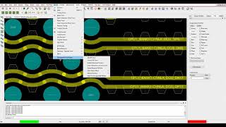
Media Summary: we can see here what are input parameter for Electrons don't just travel from just pin to pin on single layers. They can travel in the z-axis through vias and pins as well as inside ... This video will demonstrate creating several

Tutorial Cadence High Speed Tabbed - Detailed Analysis & Overview

we can see here what are input parameter for Electrons don't just travel from just pin to pin on single layers. They can travel in the z-axis through vias and pins as well as inside ... This video will demonstrate creating several

Photo Gallery

Tutorial Cadence High Speed Tabbed Routing
Allegro PCB High Speed Tabbed Routing
Tutorial Cadence PCB High Speed Analysis Coupling Workflow
Tabbed Routing High Speed Interface PCB Design
Tutorial Cadence Route Analysis Vision
Tutorial Cadence PCB High Speed Analysis Impedance Workflow
Cadence PCB High Speed Analysis Coupling Workflow
High-Speed Signal Routing : Z-Axis and Package Pin Delay | OrCAD PCB Designer
Cadence PCB Editor Timing Vision Tutorial
Creating High Speed Via Structures from with the Allegro PCB Editor
Allegro Tutorial High Speed Via Structures
Tutorial Cadence Pin Delay Z Axis
View Detailed Profile
Tutorial Cadence High Speed Tabbed Routing

Tutorial Cadence High Speed Tabbed Routing

Here we explore the

Allegro PCB High Speed Tabbed Routing

Allegro PCB High Speed Tabbed Routing

Here we explore the Allegro PCB

Tutorial Cadence PCB High Speed Analysis Coupling Workflow

Tutorial Cadence PCB High Speed Analysis Coupling Workflow

Here we explore the

Tabbed Routing High Speed Interface PCB Design

Tabbed Routing High Speed Interface PCB Design

we can see here what are input parameter for

Tutorial Cadence Route Analysis Vision

Tutorial Cadence Route Analysis Vision

Here we explore the

Tutorial Cadence PCB High Speed Analysis Impedance Workflow

Tutorial Cadence PCB High Speed Analysis Impedance Workflow

Here we explore the

Cadence PCB High Speed Analysis Coupling Workflow

Cadence PCB High Speed Analysis Coupling Workflow

here we explore the

High-Speed Signal Routing : Z-Axis and Package Pin Delay | OrCAD PCB Designer

High-Speed Signal Routing : Z-Axis and Package Pin Delay | OrCAD PCB Designer

Electrons don't just travel from just pin to pin on single layers. They can travel in the z-axis through vias and pins as well as inside ...

Cadence PCB Editor Timing Vision Tutorial

Cadence PCB Editor Timing Vision Tutorial

Here we explore the

Creating High Speed Via Structures from with the Allegro PCB Editor

Creating High Speed Via Structures from with the Allegro PCB Editor

This video will demonstrate creating several

Allegro Tutorial High Speed Via Structures

Allegro Tutorial High Speed Via Structures

Here we explore the

Tutorial Cadence Pin Delay Z Axis

Tutorial Cadence Pin Delay Z Axis

Here we explore the

Cadence PCB High Speed Analysis Impedance Workflow

Cadence PCB High Speed Analysis Impedance Workflow

Here we explore the