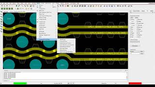
Media Summary: we can see here what are input parameter for Electrons don't just travel from just pin to pin on single layers. They can travel in the z-axis through vias and pins as well as inside ... If you are interested, you can download this PCB layout files in Altium Designer from - It's free :) Thank ...

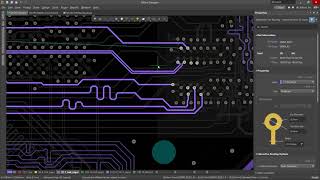
Tabbed Routing High Speed Interface - Detailed Analysis & Overview

we can see here what are input parameter for Electrons don't just travel from just pin to pin on single layers. They can travel in the z-axis through vias and pins as well as inside ... If you are interested, you can download this PCB layout files in Altium Designer from - It's free :) Thank ... In this video, see how to quickly and accurately Multidisciplinary product creation powered by your unconstrained network. Work concurrently across design, sourcing, and ... We'll look at some basic rules of thumb that apply to

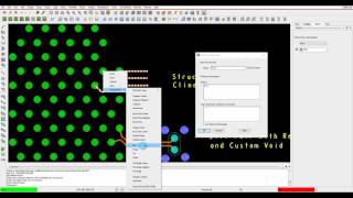
Recorded at AltiumLive 2019 Frankfurt. Pre-register for AltiumLive 2020: Here we explore the Via Structures feature in Allegro PCB Recently we've gotten a few questions about

Photo Gallery

Tabbed Routing High Speed Interface PCB Design
Tutorial Cadence High Speed Tabbed Routing
Allegro PCB High Speed Tabbed Routing
High-Speed Signal Routing : Z-Axis and Package Pin Delay | OrCAD PCB Designer
Watch routing PCB Layout with DDR3 & High Speed Interfaces
High Speed Design Overview | OrCAD PCB Designer
PADS High Speed Routing
Fast And High-Quality Routing in Altium Designer
How to Route High-Speed Designs in Altium Designer
360 LIVE: Routing for high speed designs
Routing High Speed Boards in the 5G Era
Tutorial Allegro High Speed Via Structures
View Detailed Profile
Tabbed Routing High Speed Interface PCB Design

Tabbed Routing High Speed Interface PCB Design

we can see here what are input parameter for

Tutorial Cadence High Speed Tabbed Routing

Tutorial Cadence High Speed Tabbed Routing

Here we explore the Cadence

Allegro PCB High Speed Tabbed Routing

Allegro PCB High Speed Tabbed Routing

Here we explore the Allegro PCB

High-Speed Signal Routing : Z-Axis and Package Pin Delay | OrCAD PCB Designer

High-Speed Signal Routing : Z-Axis and Package Pin Delay | OrCAD PCB Designer

Electrons don't just travel from just pin to pin on single layers. They can travel in the z-axis through vias and pins as well as inside ...

Watch routing PCB Layout with DDR3 & High Speed Interfaces

Watch routing PCB Layout with DDR3 & High Speed Interfaces

If you are interested, you can download this PCB layout files in Altium Designer from http://www.imx6rex.com/ - It's free :) Thank ...

High Speed Design Overview | OrCAD PCB Designer

High Speed Design Overview | OrCAD PCB Designer

In a

PADS High Speed Routing

PADS High Speed Routing

In this video, see how to quickly and accurately

Fast And High-Quality Routing in Altium Designer

Fast And High-Quality Routing in Altium Designer

Get

How to Route High-Speed Designs in Altium Designer

How to Route High-Speed Designs in Altium Designer

Multidisciplinary product creation powered by your unconstrained network. Work concurrently across design, sourcing, and ...

360 LIVE: Routing for high speed designs

360 LIVE: Routing for high speed designs

We'll look at some basic rules of thumb that apply to

Routing High Speed Boards in the 5G Era

Routing High Speed Boards in the 5G Era

Recorded at AltiumLive 2019 Frankfurt. Pre-register for AltiumLive 2020: https://www.altium.com/live-conference/registration.

Tutorial Allegro High Speed Via Structures

Tutorial Allegro High Speed Via Structures

Here we explore the Via Structures feature in Allegro PCB

What Are High-Speed PCBs? | Answering Your Questions!

What Are High-Speed PCBs? | Answering Your Questions!

Recently we've gotten a few questions about