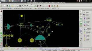
Media Summary: Deciding where the components will go 6:31 - Reference layouts. (1:20) schematic organizing rectangle, (2:00) connector schematic, (3:35) connector Learn PCB design in our new electronics and hardware PCB design course ...

Kicad Tutorial Part 4 Create - Detailed Analysis & Overview

Deciding where the components will go 6:31 - Reference layouts. (1:20) schematic organizing rectangle, (2:00) connector schematic, (3:35) connector Learn PCB design in our new electronics and hardware PCB design course ... In this comprehensive video, Peter from Tech Explorations takes you through the entire process of designing a custom IoT PCB ...

Photo Gallery

KiCAD Tutorial Part 4: Create your Symbol and Footprints + Soldering Tips
An Intro to KiCad – Part 4: Create a Footprint | DigiKey
KiCAD Custom Footprint | Part 4
KiCAD tutorial part 4 - Component Layout
Kicad Tutorial   Episode 4   Tips, Tricks
KiCad Tutorial -  How to make a 4 layer PCB in #KiCad
KiCad 7 Tutorial: Basic Operations (Part 4)
KiCAD Tutorial - Schematic Symbol and PCB Footprint Creation
Designing Eurorack Sequencer Part 4: Making a PCB with KiCad 5.0
KiCad 9.0 – Getting started Part 3: Create a Custom Schematic Symbol | DigiKey
KiCad 9: Design & assemble an ESP32 IoT 4-layer PCB loaded with goodies **A Complete Guide**
KiCAD Project Tutorial 4
View Detailed Profile
KiCAD Tutorial Part 4: Create your Symbol and Footprints + Soldering Tips

KiCAD Tutorial Part 4: Create your Symbol and Footprints + Soldering Tips

This

An Intro to KiCad – Part 4: Create a Footprint | DigiKey

An Intro to KiCad – Part 4: Create a Footprint | DigiKey

On

KiCAD Custom Footprint | Part 4

KiCAD Custom Footprint | Part 4

Creating

KiCAD tutorial part 4 - Component Layout

KiCAD tutorial part 4 - Component Layout

Deciding where the components will go 6:31 - Reference layouts.

Kicad Tutorial   Episode 4   Tips, Tricks

Kicad Tutorial Episode 4 Tips, Tricks

(1:20) schematic organizing rectangle, (2:00) connector schematic, (3:35) connector

KiCad Tutorial -  How to make a 4 layer PCB in #KiCad

KiCad Tutorial - How to make a 4 layer PCB in #KiCad

KiCad

KiCad 7 Tutorial: Basic Operations (Part 4)

KiCad 7 Tutorial: Basic Operations (Part 4)

Why

KiCAD Tutorial - Schematic Symbol and PCB Footprint Creation

KiCAD Tutorial - Schematic Symbol and PCB Footprint Creation

Learn PCB design in our new electronics and hardware PCB design course ...

Designing Eurorack Sequencer Part 4: Making a PCB with KiCad 5.0

Designing Eurorack Sequencer Part 4: Making a PCB with KiCad 5.0

In this

KiCad 9.0 – Getting started Part 3: Create a Custom Schematic Symbol | DigiKey

KiCad 9.0 – Getting started Part 3: Create a Custom Schematic Symbol | DigiKey

In

KiCad 9: Design & assemble an ESP32 IoT 4-layer PCB loaded with goodies **A Complete Guide**

KiCad 9: Design & assemble an ESP32 IoT 4-layer PCB loaded with goodies **A Complete Guide**

In this comprehensive video, Peter from Tech Explorations takes you through the entire process of designing a custom IoT PCB ...

KiCAD Project Tutorial 4

KiCAD Project Tutorial 4

Part 4

KiCAD in 3 Minutes

KiCAD in 3 Minutes

Here's a complete