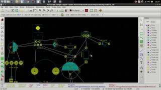
Media Summary: Learn PCB design in our new electronics and hardware PCB design course ... Start in PCB design at flux.ai Join the Flux Community: ... In this comprehensive video, Peter from Tech Explorations takes you through the entire process of designing a custom IoT PCB ...
Kicad Tutorial Part 4 Component - Detailed Analysis & Overview
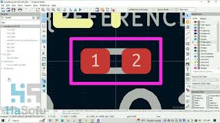
Learn PCB design in our new electronics and hardware PCB design course ... Start in PCB design at flux.ai Join the Flux Community: ... In this comprehensive video, Peter from Tech Explorations takes you through the entire process of designing a custom IoT PCB ... This video shows creating simple footprints within the