Media Summary: What is the process by which silicon is transformed into a semiconductor chip? As the second most prevalent material on earth, ... Subscribe it to get more information! Camera Module Step into the world of semiconductor manufacturing in this behind-the-scenes look at one of our 300mm
Wafer Sorting And Distribution System - Detailed Analysis & Overview
What is the process by which silicon is transformed into a semiconductor chip? As the second most prevalent material on earth, ... Subscribe it to get more information! Camera Module Step into the world of semiconductor manufacturing in this behind-the-scenes look at one of our 300mm FormFactor's ReAlign™ technology for the SUMMIT200 "Semiconductor packaging." Have you heard of it? You might be familiar with packaging, but it is one of the most important ... Applied has the industry's broadest suite of materials capabilities for fabricating devices on semiconductor
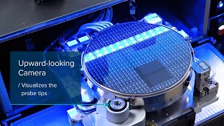
What does Technoprobe do? Probe cards, is the easy answer. But what is a probe card? Ok, this is a less easy question, but we'll ... Travel into a computer chip to explore how these devices are manufactured and what can be done about their environmental ... With due to start in less than a week, we are beyond excited to share what we're bringing to the expo this year, ... Subscribe(구독) it to get more information! [PAMTEK] Laser marking


![[PAMTEK] Laser marking system - Wafer marking & sorting : PK5210](https://i.ytimg.com/vi/g-rNQrwpHf4/mqdefault.jpg)