Media Summary: What is an atomic Lego set? What are its tiny building blocks? How can they help us create better technologies and discover ... In this animation, the next gen. of optoelectronic devices based upon the physics and tech. of layered Every day at Columbia we build nano devices by stacking atomically thin
Two Dimensional 2d Materials And - Detailed Analysis & Overview
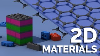
What is an atomic Lego set? What are its tiny building blocks? How can they help us create better technologies and discover ... In this animation, the next gen. of optoelectronic devices based upon the physics and tech. of layered Every day at Columbia we build nano devices by stacking atomically thin Debbie Nelson (Contributing Editor to the Nixene Journal) in conversation with Adrian Nixon (Editor in Chief of the Nixene ... In this video, Professor Humberto Terrones of Rensselaer Poytechnic Institute gives a talk on his work in You may know how buildings are built or how to make a sandwich. But what about assembling novel devices out of
Follow up to our previous video on van der Waals heterostructures, 2021.01.28 Saptarshi Das, Pennsylvania State University Table of contents available. This presentation is made available by the ... This is a 30-min seminar I gave as part of an MRS Virtual Workshop called "Next-Gen Nanotechnology Through ... 2D nanostructures, physics, chemistry, and material science of