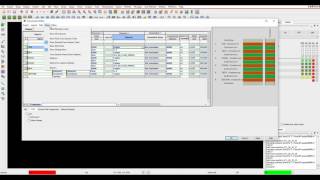
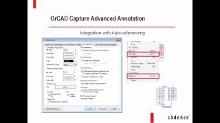
Media Summary: PCB design starts with schematic entry, part selection, circuit simulation, layout, and then system analysis. OrCAD PCB Designer ... Here we explore the different spacing constraints and classes of the With the newly introduced Advanced Annotation feature supported by OrCAD Capture, users can assign reference ranges ...
Tutorial Cadence 17 2 2016 - Detailed Analysis & Overview
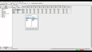
PCB design starts with schematic entry, part selection, circuit simulation, layout, and then system analysis. OrCAD PCB Designer ... Here we explore the different spacing constraints and classes of the With the newly introduced Advanced Annotation feature supported by OrCAD Capture, users can assign reference ranges ... Here we explore how to import or export IDF with Here we explore the DFM Acute Pad exit/entry rules in the Here we explore the physical constraint rules in the
Here we explore the new Cross Section Editor of the V. To enable a faster and more efficient flex and rigid-flex design creation critical to IoT, wearables and wireless devices, the OrCAD ...


![[[OrCAD 17.2Tutorial] How to intalling OrCAD 17.2 [full active]](https://i.ytimg.com/vi/M3nTag2HVXM/mqdefault.jpg)