Media Summary: Videos for competitive exams Stay tuned for more videos BEST OF LUCK TO ALL OF YOU Tricksandshortcuts ... Learn Ionic Bond in a very simple way through my video.. Follow my Channel to get latest video on chemistry related matter. Analog Circuit Design (New 2019) Professor Ali Hajimiri, Caltech Course material at: © Copyright, ...

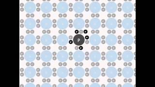
Trick In Doping Solid State - Detailed Analysis & Overview

Videos for competitive exams Stay tuned for more videos BEST OF LUCK TO ALL OF YOU Tricksandshortcuts ... Learn Ionic Bond in a very simple way through my video.. Follow my Channel to get latest video on chemistry related matter. Analog Circuit Design (New 2019) Professor Ali Hajimiri, Caltech Course material at: © Copyright, ... This video is part of the course "ECE 606: MIT 2.627 Fundamentals of Photovoltaics, Fall 2011 View the complete course: Instructor: Joe ... Dope silicon crystal with group 13 element like Boron( a trivalent element). P type semiconductor. Holes created in electric field.

Analog Integrated Circuit Design, Professor Ali Hajimiri California Institute of Technology (Caltech) Explaination of Metal excess defect or non metal deficiency defect. (F-Centre) Metal deficiency or non metal excess defect Type 3 ...

Photo Gallery

TRICK IN DOPING SOLID STATE CHEMISTRY NUMERICAL for 12TH BOARD, NEET JEE
16. Doping (Intro to Solid-State Chemistry)
LEARN DEFECTS IN  CRYSTAL || DOPING || SOLID STATE
102N. Basic Solid-State Physics: Doping, Carrier Density, Distributions
Solid state | part 9 | DOPING |
Short trick to learn all Doping elements
ECE 606 Solid State Devices L14.4: Multiple Doping, Co-Doping, And Heavy-Doping
VERY VERY IMP DOPING. SOLID STATE L-20
Tutorial: Doping
Dope silicon crystal with group 13 element like Boron. P type semiconductor. Trick to remember.
102. Basic Solid-State Physics: Holes and Electrons, Doping, Carrier Density
Doping Mechanisms in Semiconductors Explained | Solid State Devices Day 4 (B.Tech ECE)
View Detailed Profile
TRICK IN DOPING SOLID STATE CHEMISTRY NUMERICAL for 12TH BOARD, NEET JEE

TRICK IN DOPING SOLID STATE CHEMISTRY NUMERICAL for 12TH BOARD, NEET JEE

Videos for competitive exams Stay tuned for more videos BEST OF LUCK TO ALL OF YOU Tricksandshortcuts ...

16. Doping (Intro to Solid-State Chemistry)

16. Doping (Intro to Solid-State Chemistry)

MIT 3.091 Introduction to

LEARN DEFECTS IN  CRYSTAL || DOPING || SOLID STATE

LEARN DEFECTS IN CRYSTAL || DOPING || SOLID STATE

Learn Ionic Bond in a very simple way through my video.. Follow my Channel to get latest video on chemistry related matter.

102N. Basic Solid-State Physics: Doping, Carrier Density, Distributions

102N. Basic Solid-State Physics: Doping, Carrier Density, Distributions

Analog Circuit Design (New 2019) Professor Ali Hajimiri, Caltech Course material at: https://chic.caltech.edu/links/ © Copyright, ...

Solid state | part 9 | DOPING |

Solid state | part 9 | DOPING |

doping

Short trick to learn all Doping elements

Short trick to learn all Doping elements

Short trick to learn all Doping elements

ECE 606 Solid State Devices L14.4: Multiple Doping, Co-Doping, And Heavy-Doping

ECE 606 Solid State Devices L14.4: Multiple Doping, Co-Doping, And Heavy-Doping

This video is part of the course "ECE 606:

VERY VERY IMP DOPING. SOLID STATE L-20

VERY VERY IMP DOPING. SOLID STATE L-20

INTRINSIC AND EXTRINSIC SEMICONDUCTORS.

Tutorial: Doping

Tutorial: Doping

MIT 2.627 Fundamentals of Photovoltaics, Fall 2011 View the complete course: http://ocw.mit.edu/2-627F11 Instructor: Joe ...

Dope silicon crystal with group 13 element like Boron. P type semiconductor. Trick to remember.

Dope silicon crystal with group 13 element like Boron. P type semiconductor. Trick to remember.

Dope silicon crystal with group 13 element like Boron( a trivalent element). P type semiconductor. Holes created in electric field.

102. Basic Solid-State Physics: Holes and Electrons, Doping, Carrier Density

102. Basic Solid-State Physics: Holes and Electrons, Doping, Carrier Density

Analog Integrated Circuit Design, Professor Ali Hajimiri California Institute of Technology (Caltech) http://chic.caltech.edu/hajimiri/ ...

Doping Mechanisms in Semiconductors Explained | Solid State Devices Day 4 (B.Tech ECE)

Doping Mechanisms in Semiconductors Explained | Solid State Devices Day 4 (B.Tech ECE)

Welcome to Day 4 of our 40-Day

SOLID STATE #6 F-CENTRE ,DOPING, N-TYPE AND P-TYPE SEMICONDUCTOR.

SOLID STATE #6 F-CENTRE ,DOPING, N-TYPE AND P-TYPE SEMICONDUCTOR.

Explaination of Metal excess defect or non metal deficiency defect. (F-Centre) Metal deficiency or non metal excess defect Type 3 ...