Media Summary: Welcome to "Learn ADS in 5 mins" video tutorial series. In the 41st video of the tutorial series, you will learn the basics of ... AD: This video includes a paid promotion for JLCPCB.) Some tips for when Altium Develop lets your whole team — from designers to manufacturing engineers — collaborate on

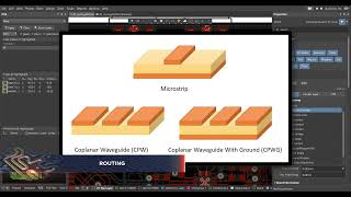
Rf Design 22 Rf Layout - Detailed Analysis & Overview

Welcome to "Learn ADS in 5 mins" video tutorial series. In the 41st video of the tutorial series, you will learn the basics of ... AD: This video includes a paid promotion for JLCPCB.) Some tips for when Altium Develop lets your whole team — from designers to manufacturing engineers — collaborate on Multidisciplinary product creation powered by your unconstrained network. Work concurrently across

Photo Gallery

RF Design-22: RF Layout Designs in ADS - Part 1
Flawless PCB design: RF rules of thumb - Part 1
Tutorial-41: Multi-Layer RF Layout Design Basics
Practical 2-Layer RF Design Rules (That Actually Work)
(Sponsored) Practical RF Hardware and PCB Design Tips - Phil's Lab #19
PCB Design Tips to Improve RF Power Amplifier Layout
RF Design in the PCB:  Routing Any angle or Arc in Altium Designer
Starting an RF PCB Design
Resolving Common Errors in RF PCB Layout Design | Sierra Circuits
RF Design-23: RF Layout Designs in ADS - Part 2
View Detailed Profile
RF Design-22: RF Layout Designs in ADS - Part 1

RF Design-22: RF Layout Designs in ADS - Part 1

Learn all about performing Schematic to

Flawless PCB design: RF rules of thumb - Part 1

Flawless PCB design: RF rules of thumb - Part 1

Full course info: https://www.hans-rosenberg.com/epdc_information_yt?utm_source=yt-d-v1 Free mini-course: ...

Tutorial-41: Multi-Layer RF Layout Design Basics

Tutorial-41: Multi-Layer RF Layout Design Basics

Welcome to "Learn ADS in 5 mins" video tutorial series. In the 41st video of the tutorial series, you will learn the basics of ...

Practical 2-Layer RF Design Rules (That Actually Work)

Practical 2-Layer RF Design Rules (That Actually Work)

Full course info: https://www.hans-rosenberg.com/epdc_information_yt?utm_source=yt-d-v3 Free mini-course: ...

(Sponsored) Practical RF Hardware and PCB Design Tips - Phil's Lab #19

(Sponsored) Practical RF Hardware and PCB Design Tips - Phil's Lab #19

AD: This video includes a paid promotion for JLCPCB.) Some tips for when

PCB Design Tips to Improve RF Power Amplifier Layout

PCB Design Tips to Improve RF Power Amplifier Layout

Altium Develop lets your whole team — from designers to manufacturing engineers — collaborate on

RF Design in the PCB:  Routing Any angle or Arc in Altium Designer

RF Design in the PCB: Routing Any angle or Arc in Altium Designer

Multidisciplinary product creation powered by your unconstrained network. Work concurrently across

Starting an RF PCB Design

Starting an RF PCB Design

Multidisciplinary product creation powered by your unconstrained network. Work concurrently across

Resolving Common Errors in RF PCB Layout Design | Sierra Circuits

Resolving Common Errors in RF PCB Layout Design | Sierra Circuits

RF PCB layout design

RF Design-23: RF Layout Designs in ADS - Part 2

RF Design-23: RF Layout Designs in ADS - Part 2

Learn how to perform