Media Summary: PCB Design Tutorial_51 Orcad Pcb Editor Design Rule Check Drc Cleanup PCB Design Tutorial_55 Orcad Pcb Editor_Delete Unconnected Shapes PCB Design Tutorial_52 Orcad Pcb Editor Artwork Film Setup
Pcb Design Tutorial 55 Orcad - Detailed Analysis & Overview
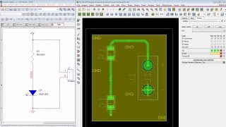
PCB Design Tutorial_51 Orcad Pcb Editor Design Rule Check Drc Cleanup PCB Design Tutorial_55 Orcad Pcb Editor_Delete Unconnected Shapes PCB Design Tutorial_52 Orcad Pcb Editor Artwork Film Setup Professor Saeid Moslehpour Video by: Jeff Roberts, Gary Claus, and Sam Alexander This video covers: -Creating component ... Sometimes we might not find schematic symbol for some components in our PCB Design Tutorial_25 Orcad Pcb Editor Custom Part 01 Footprint Creation
For everyone who would like to learn how to start with In this video it is shown, how to create a through hole DIP and a SMD SOIC footprint using the 'Package Symbol Wizard' in ...


![[OrCad Layout Plus PCB Tutorial] - Pulse generation circuit with 555 - part 1](https://i.ytimg.com/vi/4NSLjJCGsVc/mqdefault.jpg)