Media Summary: PCB Design Tutorial_53 Orcad Pcb Editor Silkscreen Text Alignment PCB Design Tutorial_25 Orcad Pcb Editor Custom Part 01 Footprint Creation PCB Design Tutorial_04- Orcad Project File Creation
Pcb Design Tutorial 53 Orcad - Detailed Analysis & Overview
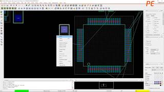
PCB Design Tutorial_53 Orcad Pcb Editor Silkscreen Text Alignment PCB Design Tutorial_25 Orcad Pcb Editor Custom Part 01 Footprint Creation PCB Design Tutorial_04- Orcad Project File Creation PCB Design Tutorial_17 Orcad Sch Part Properties Edit Sometimes we might not find schematic symbol for some components in our PCB Design Tutorial_43 Orcad Pcb Editor Component Placement 02
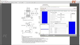
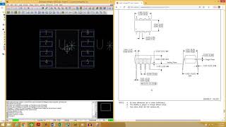
In this video it is shown, how to create a through hole DIP and a SMD SOIC footprint using the 'Package Symbol Wizard' in ... PCB Design Tutorial_35 Orcad Sch Netlist Creation PCB Design Tutorial_07-Orcad Local Library Creation