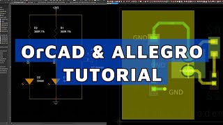
Media Summary: PCB Design Tutorial_37 Orcad Pcb Editor Netlist Import And Error Correction 01 PCB Design Tutorial_25 Orcad Pcb Editor Custom Part 01 Footprint Creation Professor Saeid Moslehpour Video by: Jeff Roberts, Gary Claus, and Sam Alexander This video covers: -Creating component ...
Pcb Design Tutorial 37 Orcad - Detailed Analysis & Overview
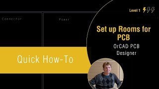
PCB Design Tutorial_37 Orcad Pcb Editor Netlist Import And Error Correction 01 PCB Design Tutorial_25 Orcad Pcb Editor Custom Part 01 Footprint Creation Professor Saeid Moslehpour Video by: Jeff Roberts, Gary Claus, and Sam Alexander This video covers: -Creating component ... In this video, we'll provide an in-depth explanation on how to configure and create rooms for component placement for efficient ... PCB Design Tutorial_07-Orcad Local Library Creation ... you'll understand how part pin numbers and names are associated with footprints uh and schematic symbols in
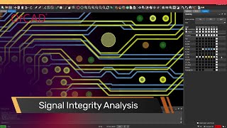
PCB Design Tutorial_17 Orcad Sch Part Properties Edit Maintaining the signal integrity (SI) of your high-speed A schematic consists of multiple circuits and blocks on multiple pages. There can be a power section, memory bus section, RF and ... For everyone who would like to learn how to start with