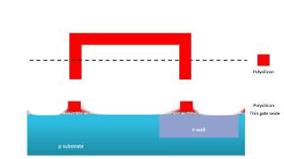
Media Summary: In this video we will discuss about p-well CMOS Lambda Based Design Rule. You can JOIN US by sign up by clicking on this ... Mr. S. P. Swami Assistant Professor Department of Electronics and Telecommunication Walchand Institute of Technology, ... Welcome back, students! In today's video, we are breaking down the

P Well Cmos Lambda Based - Detailed Analysis & Overview

In this video we will discuss about p-well CMOS Lambda Based Design Rule. You can JOIN US by sign up by clicking on this ... Mr. S. P. Swami Assistant Professor Department of Electronics and Telecommunication Walchand Institute of Technology, ... Welcome back, students! In today's video, we are breaking down the This video explains the need for design rules in VLSI. It elaborates on the

Photo Gallery

CMOS Lambda Based Design Rules || VLSI Design || S VIJAY MURUGAN || LEARN THOUGHT
Layout of CMOS INVERTER using P-WELL Process || Explore the way
P-well CMOS Lambda-Based Design Rules
P-Well CMOS Process Challenges Explained SIMPLY! | VLSI Design Basics || EC Academy
Mask layout  | Lambda based design rules | VLSI | Lec-32
CMOS Lambda design rules
CMOS Fabrication Process (Animation)
CMOS LAMBDA BASED DESIGN RULES
6 Lambda Based P Well Design Rules Explained Module 2 6th Sem VLSI ECE VTU
CMOS P-Well Fabrication Process Explained Step-by-Step | VLSI Design || EC Academy
CMOS Transistor | P-Well fabrication | VLSI | Lec-09
LAMBDA RULES
View Detailed Profile
CMOS Lambda Based Design Rules || VLSI Design || S VIJAY MURUGAN || LEARN THOUGHT

CMOS Lambda Based Design Rules || VLSI Design || S VIJAY MURUGAN || LEARN THOUGHT

This video help to learn

Layout of CMOS INVERTER using P-WELL Process || Explore the way

Layout of CMOS INVERTER using P-WELL Process || Explore the way

Layout of

P-well CMOS Lambda-Based Design Rules

P-well CMOS Lambda-Based Design Rules

In this video we will discuss about p-well CMOS Lambda Based Design Rule. You can JOIN US by sign up by clicking on this ...

P-Well CMOS Process Challenges Explained SIMPLY! | VLSI Design Basics || EC Academy

P-Well CMOS Process Challenges Explained SIMPLY! | VLSI Design Basics || EC Academy

P

Mask layout  | Lambda based design rules | VLSI | Lec-32

Mask layout | Lambda based design rules | VLSI | Lec-32

VLSI

CMOS Lambda design rules

CMOS Lambda design rules

Mr. S. P. Swami Assistant Professor Department of Electronics and Telecommunication Walchand Institute of Technology, ...

CMOS Fabrication Process (Animation)

CMOS Fabrication Process (Animation)

CMOS Fabrication Process (Animation)

CMOS LAMBDA BASED DESIGN RULES

CMOS LAMBDA BASED DESIGN RULES

cmos

6 Lambda Based P Well Design Rules Explained Module 2 6th Sem VLSI ECE VTU

6 Lambda Based P Well Design Rules Explained Module 2 6th Sem VLSI ECE VTU

PDF Notes:https://sub2unlock.io/glW5O HOW TO DOWNLOAD  ...

CMOS P-Well Fabrication Process Explained Step-by-Step | VLSI Design || EC Academy

CMOS P-Well Fabrication Process Explained Step-by-Step | VLSI Design || EC Academy

Welcome back, students! In today's video, we are breaking down the

CMOS Transistor | P-Well fabrication | VLSI | Lec-09

CMOS Transistor | P-Well fabrication | VLSI | Lec-09

VLSI

LAMBDA RULES

LAMBDA RULES

This video explains the need for design rules in VLSI. It elaborates on the

Lambda Based Design Rules for Mask Layout | VLSI Design Rules Explained | CMOS Layout | EC Academy

Lambda Based Design Rules for Mask Layout | VLSI Design Rules Explained | CMOS Layout | EC Academy

Learn