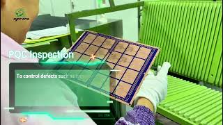
Media Summary: Join us in this comprehensive tutorial as we walk you through 33 detailed steps of producing a reliable multilayer printed circuit ... Get ready for Part 2 of our PCB Manufacturing Series! Ever wondered about the pros and cons of positive vs. negative film ... From raw copper to defined circuitry — this is where ideas become reality. At SprintPCB, our

Outer Layer Developing How To - Detailed Analysis & Overview

Join us in this comprehensive tutorial as we walk you through 33 detailed steps of producing a reliable multilayer printed circuit ... Get ready for Part 2 of our PCB Manufacturing Series! Ever wondered about the pros and cons of positive vs. negative film ... From raw copper to defined circuitry — this is where ideas become reality. At SprintPCB, our Just like in step two, this step also involves applying another photoresist to the PCB panel.

Photo Gallery

Outer layer Developing | How to make a PCB step 6.2
Outer Layer Image Developing丨Multi-layer PCB Manufacturing Process
PCB Manufacturing Process Series🎞 - Episode 2: Outer Layer Process
🌐 Outer Layer Circuit Imaging — Where Precision Begins
PCB Journey Episode 7, Outer Layer
How PCB Outer Layer Circuits Are Made | Precision Manufacturing Process
Part 13 - Image the outer layers
PCB Manufacturing Process: Outer Layer Etching
How Precision PCBs Are Made: Outer Layer Exposure & Quality Control
PCB Manufacturing Process: Outer Layer Imaging
PCB Outer Layer Development - Defining Circuit Traces with Precision.
China PCB Manufacturer丨Outer Layer Image Exposure
View Detailed Profile
Outer layer Developing | How to make a PCB step 6.2

Outer layer Developing | How to make a PCB step 6.2

Join us in this comprehensive tutorial as we walk you through 33 detailed steps of producing a reliable multilayer printed circuit ...

Outer Layer Image Developing丨Multi-layer PCB Manufacturing Process

Outer Layer Image Developing丨Multi-layer PCB Manufacturing Process

Outer Layer

PCB Manufacturing Process Series🎞 - Episode 2: Outer Layer Process

PCB Manufacturing Process Series🎞 - Episode 2: Outer Layer Process

Get ready for Part 2 of our PCB Manufacturing Series! Ever wondered about the pros and cons of positive vs. negative film ...

🌐 Outer Layer Circuit Imaging — Where Precision Begins

🌐 Outer Layer Circuit Imaging — Where Precision Begins

From raw copper to defined circuitry — this is where ideas become reality. At SprintPCB, our

PCB Journey Episode 7, Outer Layer

PCB Journey Episode 7, Outer Layer

The

How PCB Outer Layer Circuits Are Made | Precision Manufacturing Process

How PCB Outer Layer Circuits Are Made | Precision Manufacturing Process

Take a close look inside the PCB

Part 13 - Image the outer layers

Part 13 - Image the outer layers

We image the

PCB Manufacturing Process: Outer Layer Etching

PCB Manufacturing Process: Outer Layer Etching

Outer layer

How Precision PCBs Are Made: Outer Layer Exposure & Quality Control

How Precision PCBs Are Made: Outer Layer Exposure & Quality Control

Building a flawless multi-

PCB Manufacturing Process: Outer Layer Imaging

PCB Manufacturing Process: Outer Layer Imaging

Just like in step two, this step also involves applying another photoresist to the PCB panel.

PCB Outer Layer Development - Defining Circuit Traces with Precision.

PCB Outer Layer Development - Defining Circuit Traces with Precision.

PCB

China PCB Manufacturer丨Outer Layer Image Exposure

China PCB Manufacturer丨Outer Layer Image Exposure

China PCB Manufacturer丨

Outer layer AOI | How to make a PCB step 6.5

Outer layer AOI | How to make a PCB step 6.5

Join us in this comprehensive tutorial as we walk you through 33 detailed steps of producing a reliable multilayer printed circuit ...