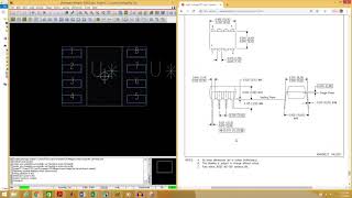
View Detailed Profile
Tutorial OrCAD and Cadence Allegro PCB Editor | 2022 | Step by Step | For Beginners

Tutorial OrCAD and Cadence Allegro PCB Editor | 2022 | Step by Step | For Beginners

After this

OrCAD Simple PCB Design Tutorial 17.4

OrCAD Simple PCB Design Tutorial 17.4

Here we explore a very simple

Cadence OrCad PCB Editor 17.4 (Complete board layout in 30 min)

Cadence OrCad PCB Editor 17.4 (Complete board layout in 30 min)

Complete

Shape Creation and Management | OrCAD PCB Designer

Shape Creation and Management | OrCAD PCB Designer

As boards gets more compact, as

Complete PCB Design Course in OrCAD and Allegro 17.4 | OrCAD & Allegro PCB Design by LtlBiTech

Complete PCB Design Course in OrCAD and Allegro 17.4 | OrCAD & Allegro PCB Design by LtlBiTech

To join our professional online course: https://pradeip009.wixsite.com/

Orcad PCB Design Tutorial - 4 Setting up the pcb environment in Orcad Allegro

Orcad PCB Design Tutorial - 4 Setting up the pcb environment in Orcad Allegro

In this video I am going to show you how to set up the

Cadence OrCad PCB Editor 17.4 (Creating Custom Footprints)

Cadence OrCad PCB Editor 17.4 (Creating Custom Footprints)

Explore the process of making a custom

OrCAD Allegro PCB Tutorial - 04: Capturing Netlists for Effective Design Integration

OrCAD Allegro PCB Tutorial - 04: Capturing Netlists for Effective Design Integration

In the

High Speed Design Overview | OrCAD PCB Designer

High Speed Design Overview | OrCAD PCB Designer

In a high-speed

How to Route Your PCB in OrCAD PCB Editor 17.4

How to Route Your PCB in OrCAD PCB Editor 17.4

This

OrCAD Basic PCB Design Tutorial Part 4 of 6

OrCAD Basic PCB Design Tutorial Part 4 of 6

Here Allah girl sorry -

Orcad PCB Design Tutorial - 10 Create smd and through hole footprint

Orcad PCB Design Tutorial - 10 Create smd and through hole footprint

In this video it is shown, how to create a through hole DIP and a SMD SOIC footprint using the 'Package Symbol Wizard' in ...