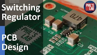
Media Summary: How to layout and route a switching regulator (buck converter in this example) using Altium Designer. Best practices, tips, and ... Thanks PCBWay for sponsoring this video - - Use this link for $5 new user free credit. Complete ... printedcircuitboard Established in 2004, Ucreate is a highly professional and experienced

Lab 7 Pcb Double Layer - Detailed Analysis & Overview

How to layout and route a switching regulator (buck converter in this example) using Altium Designer. Best practices, tips, and ... Thanks PCBWay for sponsoring this video - - Use this link for $5 new user free credit. Complete ... printedcircuitboard Established in 2004, Ucreate is a highly professional and experienced

Photo Gallery

Lab 7 PCB Double Layer-Circuit Maker
2-Layer PCB Design Tips - Phil's Lab #137
KiCad 7 STM32 Bluetooth Hardware Design (2/2 PCB) - Phil's Lab #128
Switching Regulator PCB Design - Phil's Lab #60
Making double layer PCBs at home
KiCad  7 ESP32 PCB Design Full Tutorial - made by morten laboratories iot-thing
KiCAD 7 PCB Layout in 5 steps
Lab 7 PCB Design Library and Schematic
KiCad 7 STM32 Bluetooth Hardware Design (1/2 Schematic) - Phil's Lab #127
How It's Made: Multilayer PCB Manufacturing Insight
Basic KiCad 2-Layer PCB Routing Demonstration
View Detailed Profile
Lab 7 PCB Double Layer-Circuit Maker

Lab 7 PCB Double Layer-Circuit Maker

Creating a

2-Layer PCB Design Tips - Phil's Lab #137

2-Layer PCB Design Tips - Phil's Lab #137

Tips for designing with only

KiCad 7 STM32 Bluetooth Hardware Design (2/2 PCB) - Phil's Lab #128

KiCad 7 STM32 Bluetooth Hardware Design (2/2 PCB) - Phil's Lab #128

Step-by-step schematic and

Switching Regulator PCB Design - Phil's Lab #60

Switching Regulator PCB Design - Phil's Lab #60

How to layout and route a switching regulator (buck converter in this example) using Altium Designer. Best practices, tips, and ...

Making double layer PCBs at home

Making double layer PCBs at home

Small tutorial, how to make

KiCad  7 ESP32 PCB Design Full Tutorial - made by morten laboratories iot-thing

KiCad 7 ESP32 PCB Design Full Tutorial - made by morten laboratories iot-thing

Thanks PCBWay for sponsoring this video - https://pcbway.com/g/i8683S - Use this link for $5 new user free credit. Complete ...

KiCAD 7 PCB Layout in 5 steps

KiCAD 7 PCB Layout in 5 steps

In this video we will make a

Lab 7 PCB Design Library and Schematic

Lab 7 PCB Design Library and Schematic

Computer Aided Design, Multisim.

KiCad 7 STM32 Bluetooth Hardware Design (1/2 Schematic) - Phil's Lab #127

KiCad 7 STM32 Bluetooth Hardware Design (1/2 Schematic) - Phil's Lab #127

Step-by-step schematic and

How It's Made: Multilayer PCB Manufacturing Insight

How It's Made: Multilayer PCB Manufacturing Insight

printedcircuitboard #pcbfactory #pcbmanufacturer Established in 2004, Ucreate is a highly professional and experienced

Basic KiCad 2-Layer PCB Routing Demonstration

Basic KiCad 2-Layer PCB Routing Demonstration

A basic overview of a