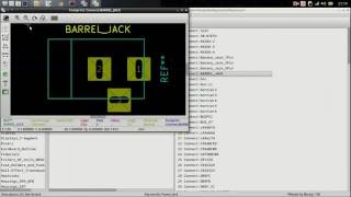
Media Summary: Learn more at HTM-Workshop.com Ready to take your This is a very simple project to demonstrate the entire process from start to finish. It is meant to be a complete overview of the ... Matching schematic symbols up to the appropriate footprints. Some of these get changed later on. This is the most "skippable" ...

Kicad Tutorial Part 2 Placing - Detailed Analysis & Overview

Learn more at HTM-Workshop.com Ready to take your This is a very simple project to demonstrate the entire process from start to finish. It is meant to be a complete overview of the ... Matching schematic symbols up to the appropriate footprints. Some of these get changed later on. This is the most "skippable" ... Okay a guy is for manufacturing so that will just show up in our drawings layer is what kind of For best development boards / components shop here : You can directly support us on Pateron ... Start in PCB design at flux.ai Join the Flux Community: ...

Photo Gallery

KiCad Tutorial Part 2 - Placing Components On Schematic Sheet
KiCad 9.0 – Getting Started Part 2: Schematic Layout | DigiKey
KiCad Tutorial Part 2 | PCB Editor Complete Beginner Guide #tutorial
KiCad Tutorial #2 Netlist and footprint association. Placing PCB items.
KiCad Custom Parts | Part 2
KiCAD 9 tutorial course [02] - Simple project
Basic KiCad 2-Layer PCB Routing Demonstration
KiCAD tutorial part 2 - Footprint Association
Kicad tutorial 2
Unofficial Buck Converter KiCAD Tutorial Part 2: Layout
Received PCB From Various Manufacturers - KiCad 7 tutorial series #pcb #electronics
Where to actually learn PCB design
View Detailed Profile
KiCad Tutorial Part 2 - Placing Components On Schematic Sheet

KiCad Tutorial Part 2 - Placing Components On Schematic Sheet

Numato Lab's

KiCad 9.0 – Getting Started Part 2: Schematic Layout | DigiKey

KiCad 9.0 – Getting Started Part 2: Schematic Layout | DigiKey

In

KiCad Tutorial Part 2 | PCB Editor Complete Beginner Guide #tutorial

KiCad Tutorial Part 2 | PCB Editor Complete Beginner Guide #tutorial

In

KiCad Tutorial #2 Netlist and footprint association. Placing PCB items.

KiCad Tutorial #2 Netlist and footprint association. Placing PCB items.

Tutorial

KiCad Custom Parts | Part 2

KiCad Custom Parts | Part 2

Learn more at HTM-Workshop.com Ready to take your

KiCAD 9 tutorial course [02] - Simple project

KiCAD 9 tutorial course [02] - Simple project

This is a very simple project to demonstrate the entire process from start to finish. It is meant to be a complete overview of the ...

Basic KiCad 2-Layer PCB Routing Demonstration

Basic KiCad 2-Layer PCB Routing Demonstration

A basic overview of a

KiCAD tutorial part 2 - Footprint Association

KiCAD tutorial part 2 - Footprint Association

Matching schematic symbols up to the appropriate footprints. Some of these get changed later on. This is the most "skippable" ...

Kicad tutorial 2

Kicad tutorial 2

covering the basic: pcbnew.

Unofficial Buck Converter KiCAD Tutorial Part 2: Layout

Unofficial Buck Converter KiCAD Tutorial Part 2: Layout

Okay a guy is for manufacturing so that will just show up in our drawings layer is what kind of

Received PCB From Various Manufacturers - KiCad 7 tutorial series #pcb #electronics

Received PCB From Various Manufacturers - KiCad 7 tutorial series #pcb #electronics

For best development boards / components shop here : https://shop.pcbcupid.com You can directly support us on Pateron ...

Where to actually learn PCB design

Where to actually learn PCB design

Start in PCB design at flux.ai Join the Flux Community: ...

KiCAD in 3 Minutes

KiCAD in 3 Minutes

Here's a complete