Media Summary: printedcircuitboard Established in 2004, Ucreate is a highly professional and experienced Get a lifetime subscription to Nebula forever at Or get a regular annual subscription ... You can watch this without ads on my streaming platform, Nebula!
Inside The Pcb Imaging Process - Detailed Analysis & Overview
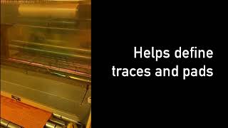
printedcircuitboard Established in 2004, Ucreate is a highly professional and experienced Get a lifetime subscription to Nebula forever at Or get a regular annual subscription ... You can watch this without ads on my streaming platform, Nebula! Just like in step two, this step also involves applying another photoresist to the