Media Summary: International SPM Symposium on Failure Analysis and Material Testing - FAMT 2021 Speaker: William Courbat, A webinar on “Nanoscale Manipulation and Probing in the SEM” organized by This presentation has been held by Prof. Ton van Helvoort at NTNU Throndheim, Norway (www.ntnu.edu) during the
Imina Technologies Sa Semiconductor Defect - Detailed Analysis & Overview
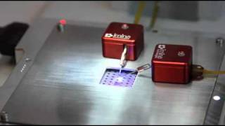
International SPM Symposium on Failure Analysis and Material Testing - FAMT 2021 Speaker: William Courbat, A webinar on “Nanoscale Manipulation and Probing in the SEM” organized by This presentation has been held by Prof. Ton van Helvoort at NTNU Throndheim, Norway (www.ntnu.edu) during the Assisted probing of LED chips with miBot micromanipulators and an XY nanopositioning stage. The process is fast and intuitive ... Imina Technologies: Probe sation semi automatic wafer testing AI is exceptionally good at spotting anomalies in
What is the process by which silicon is transformed into a This video illustrates an automated sequence in which two piezo based nanoprobers are operated to electrically contact micron ... Thanks to Ben M. for suggesting this topic and also patiently walking me through the automated optical inspection industry. The International Symposium on Testing and Failure Analysis (ISTFA), sponsored by EDFAS, creates a unique business venue for ...