Media Summary: हेलो व आर डिस्कसिंग अबाउट गेट हेलो वर डिस्कसिंग अबाउट गेट हेलो हेलो वेयर डिस्कसिंग अबाउट गेट

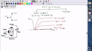
Gate 1998 Ece Jfet Biasing - Detailed Analysis & Overview

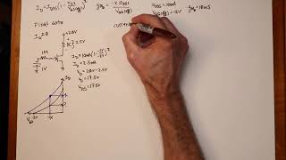
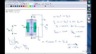
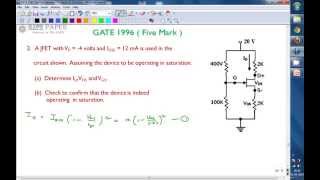
हेलो व आर डिस्कसिंग अबाउट गेट हेलो वर डिस्कसिंग अबाउट गेट हेलो हेलो वेयर डिस्कसिंग अबाउट गेट हेलो व आर डिस्कसिंग अबाउ गेट GATE 1995 ECE JFET pinch off voltage, transconductance and transit time GATE 1996 ECE JFET Biasing and Q point calculation

Photo Gallery

GATE 1998 ECE JFET Biasing
GATE 1998 ECE Transconductance and drain resistance of composite FET
Solution to GATE 1998 Electronic Devices (Five Mark) - Problem on JFET
Semiconductor Devices: JFET Biasing
JFETs: Biasing
Question on FET Transconductance - GATE 1998 ECE - (Electronic Devices) - (www.egate.ws)
GATE 1992 ECE Problem on JFET biasing
GATE 1998 ECE V - I characteristic of PN junction is a straight line when the plot is of
GATE 1995 ECE JFET pinch off voltage, transconductance and transit time
GATE 1996 ECE JFET Biasing and Q point calculation
Working of JFET (Negative Voltage at the Gate)
GATE 1987 ECE JFET pinchoff condition
View Detailed Profile
GATE 1998 ECE JFET Biasing

GATE 1998 ECE JFET Biasing

हेलो व आर डिस्कसिंग अबाउट गेट

GATE 1998 ECE Transconductance and drain resistance of composite FET

GATE 1998 ECE Transconductance and drain resistance of composite FET

हेलो वर डिस्कसिंग अबाउट गेट

Solution to GATE 1998 Electronic Devices (Five Mark) - Problem on JFET

Solution to GATE 1998 Electronic Devices (Five Mark) - Problem on JFET

हेलो हेलो वेयर डिस्कसिंग अबाउट गेट

Semiconductor Devices: JFET Biasing

Semiconductor Devices: JFET Biasing

A tour of various DC

JFETs: Biasing

JFETs: Biasing

Covers the operating regions of

Question on FET Transconductance - GATE 1998 ECE - (Electronic Devices) - (www.egate.ws)

Question on FET Transconductance - GATE 1998 ECE - (Electronic Devices) - (www.egate.ws)

EGATE - Video Solutions for previous

GATE 1992 ECE Problem on JFET biasing

GATE 1992 ECE Problem on JFET biasing

GATE 1992 ECE Problem on JFET biasing

GATE 1998 ECE V - I characteristic of PN junction is a straight line when the plot is of

GATE 1998 ECE V - I characteristic of PN junction is a straight line when the plot is of

हेलो व आर डिस्कसिंग अबाउ गेट

GATE 1995 ECE JFET pinch off voltage, transconductance and transit time

GATE 1995 ECE JFET pinch off voltage, transconductance and transit time

GATE 1995 ECE JFET pinch off voltage, transconductance and transit time

GATE 1996 ECE JFET Biasing and Q point calculation

GATE 1996 ECE JFET Biasing and Q point calculation

GATE 1996 ECE JFET Biasing and Q point calculation

Working of JFET (Negative Voltage at the Gate)

Working of JFET (Negative Voltage at the Gate)

Analog Electronics: Working of

GATE 1987 ECE JFET pinchoff condition

GATE 1987 ECE JFET pinchoff condition

Hello we are discussing about

GATE 1990 ECE Pinch off voltage of JFET

GATE 1990 ECE Pinch off voltage of JFET

GATE 1990 ECE Pinch off voltage of JFET