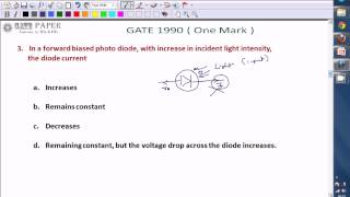
Media Summary: हेलो वी आर डिस्कसिंग अबाउट गेट in a semiconductor, under high electric fields, with increasing electric fields, mobility of charge carriers reduces and velocity of ... GATE 2010 ECE As doping on both sides of a PN junction increases,
Gate 1990 Ece Diode Doping - Detailed Analysis & Overview
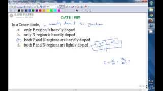
हेलो वी आर डिस्कसिंग अबाउट गेट in a semiconductor, under high electric fields, with increasing electric fields, mobility of charge carriers reduces and velocity of ... GATE 2010 ECE As doping on both sides of a PN junction increases, हेलो वी आर डिस्कसिंग अबाउट गेट ईसी पेपर GATE 1994 ECE Conductivity of p type and n type semiconductor with same doping GATE 1989 ECE In a zener diode, both P and N regions are heavily doped