Media Summary: Understanding The FinFet Semiconductor Process In this edition of Semi 101, we explore the evolution of transistor architectures that have enabled logic scaling. From the basics of ... ... 9:54 Process Node Cell Libraries 13:31 How Fin Depopulation works 14:48

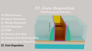
Finfet Process Flow - Detailed Analysis & Overview

Understanding The FinFet Semiconductor Process In this edition of Semi 101, we explore the evolution of transistor architectures that have enabled logic scaling. From the basics of ... ... 9:54 Process Node Cell Libraries 13:31 How Fin Depopulation works 14:48 Driven by the growing demand for increased communication and increased mobile and server data traffic, CMOS technologies ... Applied Materials engineers have been working with our customers for many years to develop the key materials engineering ... This is a Flash animation of the fabrication

Presented at SISPAD 2013 T2E-CAD: Linking Samsung's patented version of Gate-All-Around, MBCFET™ (Multi-Bridge-Channel FET), uses a nanosheet architecture, which ...

Photo Gallery

FinFET process flow
Understanding The FinFet Semiconductor Process
Gate-All-Around, Transistor Architecture Designed for the Future of Logic Devices (Semi 101)
FinFET Process Lecture
TSMC FinFlex: How Chips are made Worse to get Better
Advanced Process Technologies - Part 2: Fabricating a FinFET
FinFET
Lecture 39 Introduction to FinFETs Structure
Engineering the Gate-All-Around Transistor
Semitracks: Intel Ivy Bridge 22nm FinFET Process Fabrication
FinFETs
FinFET Technology (Basics, Structure, Characteristics, Merits, Demerits & Applications) Explained
View Detailed Profile
FinFET process flow

FinFET process flow

Preparation of substrate ...

Understanding The FinFet Semiconductor Process

Understanding The FinFet Semiconductor Process

Understanding The FinFet Semiconductor Process

Gate-All-Around, Transistor Architecture Designed for the Future of Logic Devices (Semi 101)

Gate-All-Around, Transistor Architecture Designed for the Future of Logic Devices (Semi 101)

In this edition of Semi 101, we explore the evolution of transistor architectures that have enabled logic scaling. From the basics of ...

FinFET Process Lecture

FinFET Process Lecture

Lecture on the 14nm

TSMC FinFlex: How Chips are made Worse to get Better

TSMC FinFlex: How Chips are made Worse to get Better

... 9:54 Process Node Cell Libraries 13:31 How Fin Depopulation works 14:48

Advanced Process Technologies - Part 2: Fabricating a FinFET

Advanced Process Technologies - Part 2: Fabricating a FinFET

This is part 2 of my lecture on Advanced

FinFET

FinFET

Driven by the growing demand for increased communication and increased mobile and server data traffic, CMOS technologies ...

Lecture 39 Introduction to FinFETs Structure

Lecture 39 Introduction to FinFETs Structure

This lecture introduces

Engineering the Gate-All-Around Transistor

Engineering the Gate-All-Around Transistor

Applied Materials engineers have been working with our customers for many years to develop the key materials engineering ...

Semitracks: Intel Ivy Bridge 22nm FinFET Process Fabrication

Semitracks: Intel Ivy Bridge 22nm FinFET Process Fabrication

This is a Flash animation of the fabrication

FinFETs

FinFETs

Presented at SISPAD 2013 T2E-CAD: Linking

FinFET Technology (Basics, Structure, Characteristics, Merits, Demerits & Applications) Explained

FinFET Technology (Basics, Structure, Characteristics, Merits, Demerits & Applications) Explained

FinFET Technology

Samsung Foundry’s New Transistor Structure: MBCFET™

Samsung Foundry’s New Transistor Structure: MBCFET™

Samsung's patented version of Gate-All-Around, MBCFET™ (Multi-Bridge-Channel FET), uses a nanosheet architecture, which ...