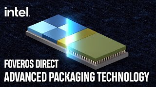
Media Summary: Part of the advanced packaging process of semiconductors includes a technology called The world's most intricate and high-tech package is one you'll likely never see. Once given little attention in chipmaking, packages ... 1. Foveros ? 2. Structure : Active interposer, Micro bump, TSV, Package on Package : Top compute die : Bottom base die 3.

Eng Sub Intel Emib - Detailed Analysis & Overview

Part of the advanced packaging process of semiconductors includes a technology called The world's most intricate and high-tech package is one you'll likely never see. Once given little attention in chipmaking, packages ... 1. Foveros ? 2. Structure : Active interposer, Micro bump, TSV, Package on Package : Top compute die : Bottom base die 3. At 66 years old, instead of heading towards retirement, former Cadence CEO and legendary investor Lip Bu Tan decided to take ... Chiplets are redefining the future of semiconductor design. Instead of building one massive monolithic chip, functions are split into ...

Photo Gallery

[Eng Sub] Intel EMIB
How Intel's EMIB technology is improving advanced chip packaging 📍| Intel
Intel Foundry EMIB | Intel
Intel EMIB Part 2 | Intel Foundry
Co-EMIB, Intel’s EMIB and Foveros Tech Together, Delivers High Bandwidth at Low Power
Intel Foundry EMIB Workflow
1  Packaging Process Technology  TSMC and Intel, CoWoS, EMIB, Foveros and Chiplets
Intel Leads the Way with Advanced Packaging
Foveros Direct: Advanced Packaging Technology to Continue Moore’s Law | Intel Technology
[Eng Sub] Intel Foveros
Intel EMIB brings new Taiwan suppliers to Google TPU as CoWoS capacity tightens
Re-engineering the Semiconductor Supply Chain with Intel CEO Lip Bu Tan
View Detailed Profile
[Eng Sub] Intel EMIB

[Eng Sub] Intel EMIB

1.

How Intel's EMIB technology is improving advanced chip packaging 📍| Intel

How Intel's EMIB technology is improving advanced chip packaging 📍| Intel

Part of the advanced packaging process of semiconductors includes a technology called

Intel Foundry EMIB | Intel

Intel Foundry EMIB | Intel

Intel's

Intel EMIB Part 2 | Intel Foundry

Intel EMIB Part 2 | Intel Foundry

Embedded Multi-die Interconnect Bridge (

Co-EMIB, Intel’s EMIB and Foveros Tech Together, Delivers High Bandwidth at Low Power

Co-EMIB, Intel’s EMIB and Foveros Tech Together, Delivers High Bandwidth at Low Power

Learn more about

Intel Foundry EMIB Workflow

Intel Foundry EMIB Workflow

EMIB

1  Packaging Process Technology  TSMC and Intel, CoWoS, EMIB, Foveros and Chiplets

1 Packaging Process Technology TSMC and Intel, CoWoS, EMIB, Foveros and Chiplets

1 Packaging Process Technology TSMC and

Intel Leads the Way with Advanced Packaging

Intel Leads the Way with Advanced Packaging

The world's most intricate and high-tech package is one you'll likely never see. Once given little attention in chipmaking, packages ...

Foveros Direct: Advanced Packaging Technology to Continue Moore’s Law | Intel Technology

Foveros Direct: Advanced Packaging Technology to Continue Moore’s Law | Intel Technology

Foveros Direct is

[Eng Sub] Intel Foveros

[Eng Sub] Intel Foveros

1. Foveros ? 2. Structure : Active interposer, Micro bump, TSV, Package on Package : Top compute die : Bottom base die 3.

Intel EMIB brings new Taiwan suppliers to Google TPU as CoWoS capacity tightens

Intel EMIB brings new Taiwan suppliers to Google TPU as CoWoS capacity tightens

Intel's EMIB

Re-engineering the Semiconductor Supply Chain with Intel CEO Lip Bu Tan

Re-engineering the Semiconductor Supply Chain with Intel CEO Lip Bu Tan

At 66 years old, instead of heading towards retirement, former Cadence CEO and legendary investor Lip Bu Tan decided to take ...

Chiplets Explained: How 2.5D & 3D Packaging Are Shaping the Future of Semiconductors

Chiplets Explained: How 2.5D & 3D Packaging Are Shaping the Future of Semiconductors

Chiplets are redefining the future of semiconductor design. Instead of building one massive monolithic chip, functions are split into ...