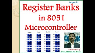
Media Summary: at 3:59 by mistake I have written 7 register in each bank but consider as shown in diagram there ... e-Learning of RAM Memory Allocation and Concept of Subject:Electronics and Communications Course:
8051 Microcontroller Register Banks Stack - Detailed Analysis & Overview
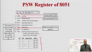
at 3:59 by mistake I have written 7 register in each bank but consider as shown in diagram there ... e-Learning of RAM Memory Allocation and Concept of Subject:Electronics and Communications Course: ch3_3:8051 microcontroller Register Banks PSW register flags_iraq In this session, I discuss the Memory organization of Myself Shridhar Mankar an Engineer l YouTuber l Educational Blogger l Educator l Podcaster. My Aim- To Make Engineering ...