Media Summary: Multidisciplinary product creation powered by your unconstrained network. Work concurrently across design, sourcing, and ... In this video I show you how to define your You can support me on Patreon here: A walk through of configuring a project

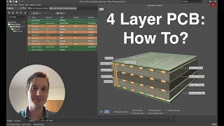
4 Layer Pcb Stackup Strategy - Detailed Analysis & Overview

Multidisciplinary product creation powered by your unconstrained network. Work concurrently across design, sourcing, and ... In this video I show you how to define your You can support me on Patreon here: A walk through of configuring a project

Photo Gallery

Signal Ground Power Ground 4-Layer Stackup? PCB Design Explained!
4-Layer PCB Stackup Strategy — SGPS, Return Currents, EMI & Controlled Impedance Explained
PCB Stack-Up and Build-Up - Phil's Lab #56
How To Define a 4 Layer PCB Stackup
Designing a 4 Layer PCB Stackup With 50 Ohm Impedance | Signal Integrity
PCB Layer Stackup basics for Beginners: A Simple Guide | 4 Layer PCB Stackup in 2025 |
KiCad 5 #20 4 Layer PCB Layout
How to choose PCB stackup?
How to Decide on Your PCB Layer Ordering, Pouring and Stackup (with Rick Hartley)
How to Create 4 Layer PCBs using Altium Easily? Altium Tutorial for Beginners
Alternative 4-layer Boards for High Speed PCBs
PCB Stackup Explained - What layer ordering is good or bad and why | Rick Hartley | #HighlightsRF
View Detailed Profile
Signal Ground Power Ground 4-Layer Stackup? PCB Design Explained!

Signal Ground Power Ground 4-Layer Stackup? PCB Design Explained!

Multidisciplinary product creation powered by your unconstrained network. Work concurrently across design, sourcing, and ...

4-Layer PCB Stackup Strategy — SGPS, Return Currents, EMI & Controlled Impedance Explained

4-Layer PCB Stackup Strategy — SGPS, Return Currents, EMI & Controlled Impedance Explained

The

PCB Stack-Up and Build-Up - Phil's Lab #56

PCB Stack-Up and Build-Up - Phil's Lab #56

What a

How To Define a 4 Layer PCB Stackup

How To Define a 4 Layer PCB Stackup

In this video I show you how to define your

Designing a 4 Layer PCB Stackup With 50 Ohm Impedance | Signal Integrity

Designing a 4 Layer PCB Stackup With 50 Ohm Impedance | Signal Integrity

Even low

PCB Layer Stackup basics for Beginners: A Simple Guide | 4 Layer PCB Stackup in 2025 |

PCB Layer Stackup basics for Beginners: A Simple Guide | 4 Layer PCB Stackup in 2025 |

Dive into the fascinating world of

KiCad 5 #20 4 Layer PCB Layout

KiCad 5 #20 4 Layer PCB Layout

You can support me on Patreon here: https://www.patreon.com/johnsbasement A walk through of configuring a project

How to choose PCB stackup?

How to choose PCB stackup?

Why is the thickness of

How to Decide on Your PCB Layer Ordering, Pouring and Stackup (with Rick Hartley)

How to Decide on Your PCB Layer Ordering, Pouring and Stackup (with Rick Hartley)

Do you pour copper on your signal

How to Create 4 Layer PCBs using Altium Easily? Altium Tutorial for Beginners

How to Create 4 Layer PCBs using Altium Easily? Altium Tutorial for Beginners

Altium Designer: A

Alternative 4-layer Boards for High Speed PCBs

Alternative 4-layer Boards for High Speed PCBs

4

PCB Stackup Explained - What layer ordering is good or bad and why | Rick Hartley | #HighlightsRF

PCB Stackup Explained - What layer ordering is good or bad and why | Rick Hartley | #HighlightsRF

Examples of 2 /

How to Setup your Multi-layer #PCBdesign - Blind and Buried Vias

How to Setup your Multi-layer #PCBdesign - Blind and Buried Vias

Set up your Layer