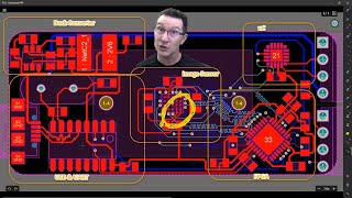
Media Summary: Creating Footprints, Adding 3D models, Updating Schematic Symbols, Annotating, Schematic Step-by-Step video for everyone ... Use ready-made electrical templates to speed up circuit planning and documentation: KiCAD Project Multidisciplinary product creation powered by your unconstrained network. Work concurrently across design, sourcing, and ...

Tutorial 2 Pcb Layout Component - Detailed Analysis & Overview

Creating Footprints, Adding 3D models, Updating Schematic Symbols, Annotating, Schematic Step-by-Step video for everyone ... Use ready-made electrical templates to speed up circuit planning and documentation: KiCAD Project Multidisciplinary product creation powered by your unconstrained network. Work concurrently across design, sourcing, and ...

Photo Gallery

Tutorial 2 for Altium Beginners: How to create footprints
Step by Step Tutorial 2 for Altium: Printed Circuit Board Layout
SparkFun According to Pete #35: PCB Layout Part 2
EEVblog #1323 - PCB Layout Review & Analysis
KiCad 9 Hardware Design Tutorial (TI MSPM0) (2/2 PCB) - Phil's Lab #166
PCB´s Design -  How to properly layout components (Part #2)
Where to actually learn PCB design
KiCAD Project PCB Layout | Part 6
Tutorial 3 for Altium Beginners: PCB Layout
KiCAD in 3 Minutes
Two-Layer PCB Design Tips: Achieving the Optimal Layout
Tutorial 2 for Eagle: Printed Circuit Board Layout
View Detailed Profile
Tutorial 2 for Altium Beginners: How to create footprints

Tutorial 2 for Altium Beginners: How to create footprints

Creating Footprints, Adding 3D models, Updating Schematic Symbols, Annotating, Schematic Step-by-Step video for everyone ...

Step by Step Tutorial 2 for Altium: Printed Circuit Board Layout

Step by Step Tutorial 2 for Altium: Printed Circuit Board Layout

Join me as I

SparkFun According to Pete #35: PCB Layout Part 2

SparkFun According to Pete #35: PCB Layout Part 2

Tags: ATP Talent: Pete Dokter.

EEVblog #1323 - PCB Layout Review & Analysis

EEVblog #1323 - PCB Layout Review & Analysis

Dave analyses a

KiCad 9 Hardware Design Tutorial (TI MSPM0) (2/2 PCB) - Phil's Lab #166

KiCad 9 Hardware Design Tutorial (TI MSPM0) (2/2 PCB) - Phil's Lab #166

Step-by-step

PCB´s Design -  How to properly layout components (Part #2)

PCB´s Design - How to properly layout components (Part #2)

The

Where to actually learn PCB design

Where to actually learn PCB design

Start in

KiCAD Project PCB Layout | Part 6

KiCAD Project PCB Layout | Part 6

Use ready-made electrical templates to speed up circuit planning and documentation: http://bit.ly/4nceY4A KiCAD Project

Tutorial 3 for Altium Beginners: PCB Layout

Tutorial 3 for Altium Beginners: PCB Layout

Starting a new

KiCAD in 3 Minutes

KiCAD in 3 Minutes

Here's a complete KiCAD

Two-Layer PCB Design Tips: Achieving the Optimal Layout

Two-Layer PCB Design Tips: Achieving the Optimal Layout

Multidisciplinary product creation powered by your unconstrained network. Work concurrently across design, sourcing, and ...

Tutorial 2 for Eagle: Printed Circuit Board Layout

Tutorial 2 for Eagle: Printed Circuit Board Layout

In this second

Basic KiCad 2-Layer PCB Routing Demonstration

Basic KiCad 2-Layer PCB Routing Demonstration

A basic overview of a